Doping a Semiconductor
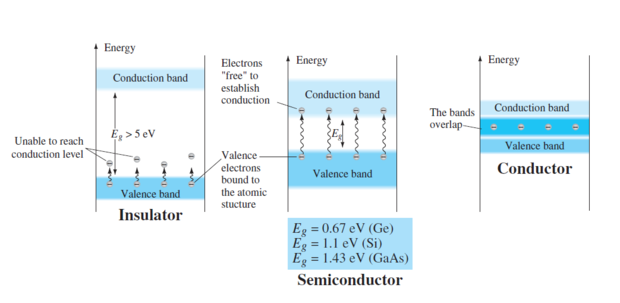
Semiconductors are generally poor conductors
Conductivity can be drastically increased by the controlled addition of impurities to the intrinsic (pure) semiconductive material
Process, called doping, increases the number of current carriers (electrons or holes)
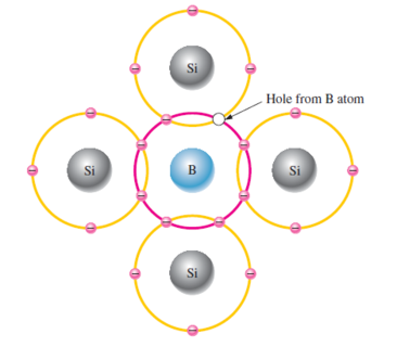
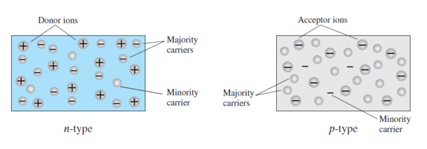
The two categories of impurities are n-type and p-type
A semiconductor material that has been subjected to the doping process is called an extrinsic material
Both n -type and p -type materials are formed by adding a predetermined number of impurity atoms to a silicon base.
N-Type Semiconductor
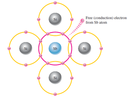
To increase the number of conduction-band electrons in intrinsic silicon, pentavalent impurity atoms are added
Atoms with five valence electrons such as arsenic (As), phosphorus (P), bismuth (Bi), and antimony (Sb).
Sb atom’s 4 valence electrons form the covalent bonds with Si atoms, leaving one extra electron
Extra electron becomes conduction electron as it is not involved in bonding.
Pentavalent atom gives up an electron, called a donor atom


