Metal-oxide-semiconductor field-effect transistor (MOSFET)s
Introduction to MOSFETs
A type of field-effect transistor (FET) used for amplification and switching.
Unlike JFETs, MOSFETs have an insulated gate separated by a silicon dioxide (SiO\(_2\)) layer.
Two main types:
Enhancement MOSFET (E-MOSFET)
Depletion MOSFET (D-MOSFET).
Polycrystalline silicon is commonly used for the gate material.
Types of MOSFETs
Enhancement MOSFET (E-MOSFET):
Operates only in enhancement mode
Requires a threshold voltage to induce a channel.
Depletion MOSFET (D-MOSFET):
Operates in both depletion and enhancement modes
Allow bidirectional control of current.
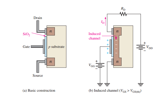
E-MOSFET - Structure & Operation
No physical channel present initially.
Applying a positive gate-to-source voltage (\(V_{GS}\)) creates an inversion layer, forming a conductive channel.
Increasing \(V_{GS}\) enhances conductivity by attracting more electrons (n-channel) or holes (p-channel).
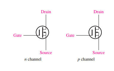
Schematic symbols: broken lines represent the absence of a structural channel.

D-MOSFET - Structure & Operation
Channel exists at zero gate voltage.
Functions as a capacitor with gate as one plate, channel as another, and SiO\(_2\) as the dielectric.

Operates in Depletion Mode when a negative \(V_{GS}\) repels electrons, reducing conductivity.
Operates in Enhancement Mode when a positive \(V_{GS}\) attracts electrons, increasing conductivity.
Operation of n-channel D-MOSFET

Comparison of E-MOSFET and D-MOSFET
| Feature | BJT | FET |
|---|---|---|
| Charge Carriers | Electrons & Holes (Bipolar) | Electrons or Holes (Unipolar) |
| Control Mechanism | Current-Controlled | Voltage-Controlled |
| Input Impedance | Low | High |
| Switching Speed | Slower | Faster |
| Preferred Applications | Amplifiers | Switching & High Impedance Circuits |
Power MOSFET Structures
Conventional E-MOSFETs: Feature a long, thin lateral channel, leading to high drain-to-source resistance, limiting power applications.

Laterally Diffused MOSFET (LDMOSFET): Has a shorter channel and lower resistance, enabling higher current and voltage applications.

VMOSFET: Features a vertical channel structure with a V-groove, allowing higher power dissipation and improved frequency response.

TMOSFET: Uses a vertical structure similar to VMOSFET but with greater packing density for better efficiency.

Dual-Gate MOSFETs
Available in both depletion and enhancement types.
Features two gates, reducing input capacitance for high-frequency applications.
Commonly used in RF amplifiers and automatic gain control (AGC) applications.
Biasing the second gate allows fine-tuning of transconductance.

E-MOSFET Transfer Characteristics
Operates only in enhancement mode, requiring a threshold voltage (\(V_{GS(th)}\)) to induce conduction.
No drain current (\(I_D\)) when \(V_{GS} = 0\), unlike JFET and D-MOSFET.
- equation: Transfer characteristic follows a\[I_D = K(V_{GS} - V_{GS(th)})^2\]
Constant \(K\) is device-specific and derived from datasheet values.

D-MOSFET Transfer Characteristics
Can operate in both depletion and enhancement modes.
- Transfer characteristic similar to JFET, obeying the square-law equation:\[V_{GS(off)} = -V_p\]
Drain current at \(V_{GS} = 0\) corresponds to \(I_{DSS}\).
For \(V_{GS} < V_{GS(off)}\), channel is fully depleted, and \(I_D = 0\).

E-MOSFET Biasing Techniques
Zero bias is not possible since V\(_{GS}\) must be greater than V\(_{GS(th)}\).
Common biasing methods:
Voltage-divider bias:
Provides a stable operating point.
Drain-feedback bias:
Provides automatic biasing with feedback stabilization.
\(V_{GS}=V_{DS}\) due to negligible gate current.

D-MOSFET Biasing Techniques
Zero-bias operation is possible (V\(_{GS}\) = 0).
Allows AC signal variations at the gate.
- Equation\[V_{DS} = V_{DD} - I_{DSS} R_{D}\]
Gate resistor (R\(_{G}\)) isolates the AC signal from ground without affecting biasing.

Applications of MOSFETs
Analog Circuits: Used in amplifiers and voltage regulators.
Digital Circuits: Integral in CMOS (Complementary MOS) technology for logic gates.
Power Electronics: Used in switching applications such as inverters and DC-DC converters.
Radio Frequency (RF) Applications: Found in communication circuits.
Conclusion
MOSFETs are crucial in modern electronics, used in digital circuits, amplifiers, and power applications.
Different MOSFET types offer flexibility in high-power and high-frequency applications.
Power MOSFETs (LDMOSFET, VMOSFET, TMOSFET) provide enhanced efficiency and performance.
Biasing techniques ensure stable operation in various applications.