Introduction to the Bipolar Junction Transistor (BJT)
Inventor: William Shockley, 1951
Purpose: Amplifies electronic signals, such as radio and TV signals
Impact: Led to inventions like the integrated circuit (IC)
Enabled the development of modern computers and electronics
Focus: Basics of BJT operation and usage as a switch
Definition: A semiconductor device that uses free electrons and holes
"Bipolar" Meaning: Refers to “two polarities” of charge carriers (electrons and holes)
Structure of an Unbiased Transistor
Three Doped Regions:
Emitter: Bottom region, heavily doped
Base: Middle region, very thin and lightly doped
Collector: Top region, intermediate doping
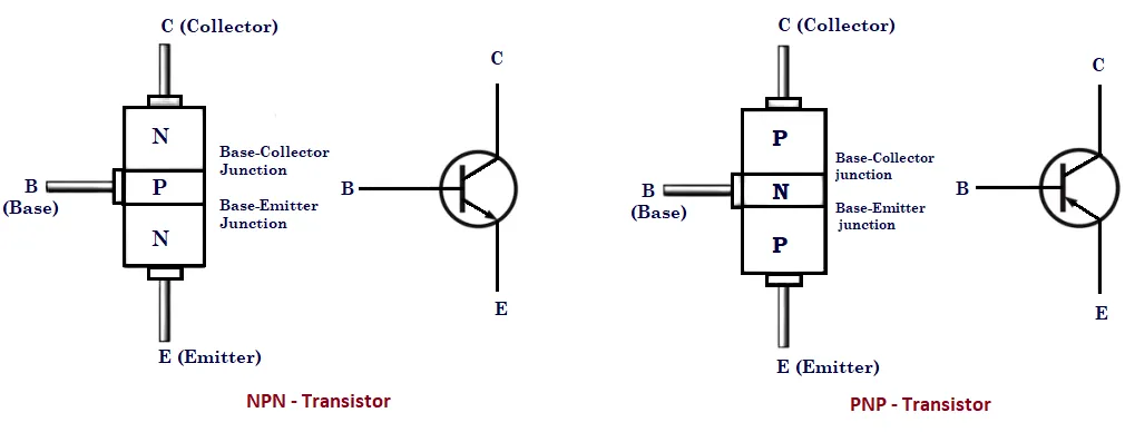
Types of Transistors:
NPN: p region between two n regions
PNP: n region between two p regions
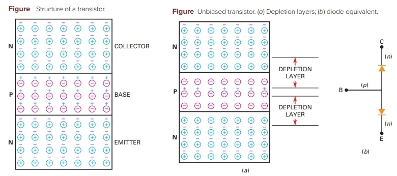
Doping Levels in a BJT
Emitter: Heavily doped for high electron flow
Base: Lightly doped for control over electron flow
Collector: Intermediate doping level, physically largest region
Emitter and Collector Diodes
Two Junctions in a BJT:
Emitter-Base Junction (or Emitter Diode)
Collector-Base Junction (or Collector Diode)
Acts like two back-to-back diodes
Before and After Diffusion in a BJT
Diffusion Process: Free electrons in n regions spread across the junction and recombine with holes in p region
Results in the formation of two depletion layers
Barrier Potential:
Silicon Transistors: Approx. 0.7 V at \(25^\circ \mathrm{C}\)
Germanium Transistors: Approx. 0.3 V at \(25^\circ \mathrm{C}\)
NPN and PNP Transistors
Key Points to Remember
BJT Structure and Operation
Importance of Doping Levels
Emitter and Collector Junctions
Formation of Depletion Layers and Barrier Potential
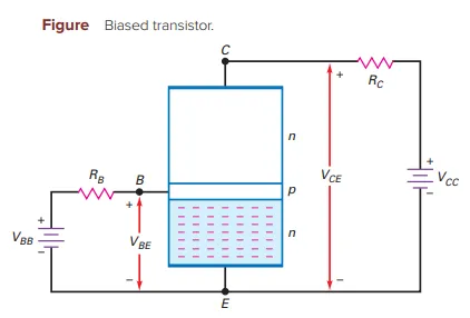
Understanding the Biased Transistor
Unbiased Transistor: Acts as two back-to-back diodes with \(\approx 0.7 ~\mathrm{V}\) barrier potential each
Important for testing NPN transistors with a DMM (Digital Multimeter)
Biased Transistor: With external voltage sources, currents flow through various transistor regions
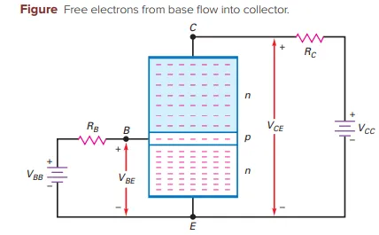
Emitter Electrons in a Biased Transistor
Purpose of the Emitter:
Heavily doped to emit free electrons into the base
Purpose of the Base:
Lightly doped to pass electrons on to the collector
Purpose of the Collector:
Collects most electrons from the base
Biasing Voltages:
\(\mathbf{V_{BB}}\): Forward-biases the emitter diode
\(\mathbf{V_{CC}}\): Reverse-biases the collector diode
Flow of Base Electrons
Action on Forward Bias (\(\mathbf{V_{BB}}\)):
When \(\mathbf{V_{BB}}>\) Barrier Potential (\(\sim\)0.7 V), emitter electrons enter the base region
Electron Flow Options:
Flow Left: Out of base through \(R_{B}\) (base resistor)
Flow Right: Into the collector
Outcome:
Most electrons move to the collector due to:
Light doping (long electron lifetime in base)
Thin base (short distance to collector)
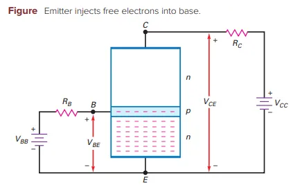
Collector Electrons and Current Flow
Collector Attraction:
\(\mathbf{V_{CC}}\) attracts free electrons into the collector region
Electron Path:
Electrons flow through \(R_C\) (collector resistor) to the positive terminal of \(\mathbf{V_{CC}}\)
Summary of Current Flow:
\(\mathbf{V_{BB}}\): Drives electrons from emitter to base
\(\mathbf{V_{CC}}\): Draws electrons through the collector and \(R_C\) to complete the circuit
Understanding Transistor Currents
Current Types in a Transistor:
Emitter Current (\(I_E\))
Base Current (\(I_B\))
Collector Current (\(I_C\))
Current Flow Representations:
Conventional Flow
Electron Flow
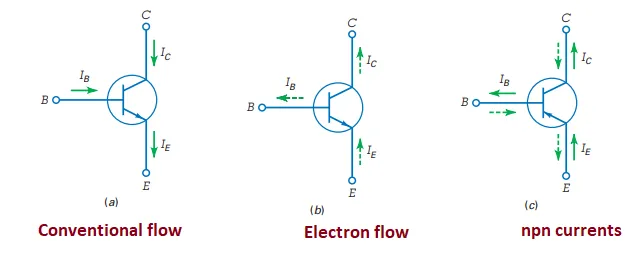
Comparison of Transistor Currents
Largest Current: Emitter current (IE), as it’s the source of electrons
Collector Current (IC): Nearly as large as IE
Base Current (IB): Much smaller, often \(<1\%\) of IC
Relation of Currents (Kirchhoff’s Current Law)
Current Relationship: \[I_E = I_C + I_B\]
Approximation (Due to small IB): \[I_C \approx I_E\] \[I_B \ll I_C\]
Application: Holds true for both NPN and PNP transistors
DC Alpha (\(\alpha\))
Definition:
Ratio of DC Collector Current to DC Emitter Current \[\alpha_{dc} = \frac{I_C}{I_E}\]
Typical Value:
Slightly \(<\)1 (Low-power: \(>0.99\), High-power: \(>0.95\))
DC Beta (\(\beta\))
Definition:
Ratio of DC Collector Current to DC Base Current \[\beta_{dc} = \frac{I_C}{I_B}\]
Current Gain:
Controls larger IC with small IB
Low-power transistors: \(\beta = 100-300\)
High-power transistors: \(\beta = 20-100\)
Using Beta to Derive Currents
Calculating Collector Current (IC): \[I_C = \beta_{dc} I_B\]
Calculating Base Current (IB): \[I_B = \frac{I_C}{\beta_{dc}}\]
Transistor Connections Overview
Three configurations:
CE (Common Emitter) – Focus of this chapter
CC (Common Collector) - Discussed later
CB (Common Base) - Discussed later
CE Connection: Most widely used.
Common Emitter Circuit
Configuration:
Emitter connected to ground.
Two loops:
Base Loop: Forward-biased by \(V_{BB}\) with \(R_B\) as the limiter.
Collector Loop: Reverse-biased by \(V_{CC}\) via \(R_C\).
Key Insight: Base current controls the collector current.
Voltage Behavior in CE Circuit
Base Loop:
Base current (\(I_B\)) generates voltage across \(R_B\).
Polarity shown
Collector Loop:
Collector current (\(I_C\)) creates voltage across \(R_C\).
Collector must remain positive for proper operation.
Double-Subscript Notation
Definition:
Same subscripts = Source voltage (e.g., \(V_{BB}\), \(V_{CC}\)).
Different subscripts = Voltage between two points (e.g., \(V_{BE}\), \(V_{CE}\)).
Measurement: Positive meter probe on first subscript. Common probe on second subscript.
Examples of Double-Subscript Voltages
Key Equations:
\(V_{CE} = V_C - V_E\)
\(V_{CB} = V_C - V_B\)
\(V_{BE} = V_B - V_E\)
In Fig. (b) (grounded circuit):
\(V_E = 0\) simplifies equations:
\(V_{CE} = V_C\)
\(V_{CB} = V_C - V_B\)
\(V_{BE} = V_B\)
Single-Subscript Notation
Node Voltages: Voltage relative to ground.
Examples in Fig. (b):
\(V_B\): Base to ground.
\(V_C\): Collector to ground.
\(V_E = 0\): Emitter to ground.
The Base Curve
Graph: \(I_B\) vs \(V_{BE}\) resembles a diode graph.
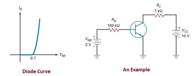
Reason: Emitter diode is forward biased.
Ohm’s Law: \[I_B = \frac{V_{BB} - V_{BE}}{R_B}\]
Approximations for \(V_{BE}\):
Ideal: \(V_{BE} = 0\)
Second: \(V_{BE} = 0.7 \, \text{V}\) (Best balance between speed and accuracy).
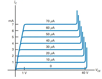
Collector Curves
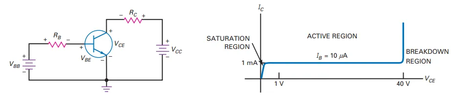
Setup: Fix \(I_B\), vary \(V_{CC}\), measure \(I_C\) and \(V_{CE}\).
Key Observations:
\(V_{CE} = 0\): No \(I_C\); diode not reverse-biased.
\(V_{CE} > 0\):
\(I_C\) rises sharply, then stabilizes (\(1 \, \text{mA}\)).
Beyond 40V: Transistor breaks down and stops working.
Significance: \(I_C\) depends on emitter injections, not \(V_{CE}\).
Collector Voltage and Power
Voltage Equation (KVL): \[V_{CE} = V_{CC} - I_C R_C\]
Power Dissipation: \[P_D = V_{CE} \cdot I_C\]
Critical Points:
Power raises junction temperature.
Burnout at \(150–200^{\circ}C\).
Ensure \(P_D < P_D(\text{max})\).
Regions of Operation
Active Region:
\(1 \, \text{V} \leq V_{CE} \leq 40 \, \text{V}\).
\(I_C\) constant, independent of \(V_{CE}\).
Emitter forward-biased, collector reverse-biased.
Saturation Region:
\(V_{CE} < 1 \, \text{V}\).
Insufficient voltage to collect all free electrons.
Lower current gain (\(\beta_{dc}\)).
Breakdown Region:
\(V_{CE} > 40 \, \text{V}\).
Transistor destroyed; avoid operation here.
Key Takeaways
Use the second diode approximation (\(V_{BE} = 0.7 \, \text{V}\)) for calculations.
Maintain \(P_D\) and \(V_{CE}\) within safe limits to avoid burnout.
Understand the active, saturation, and breakdown regions for proper transistor operation.
More Collector Curves
Second Curve (\(I_B = 20 \, \mu A\)):
\(I_C = 2 \, \text{mA}\) in the active region.
Observation: Each \(I_C\) curve corresponds to \(I_C = \beta_{dc} \cdot I_B\).
For example: \[\beta_{dc} = \frac{I_C}{I_B} = \frac{7 \, \text{mA}}{70 \, \mu \text{A}} = 100\]
Key Point: \(\beta_{dc}\) is constant for all curves in the active region.
Measurement: Use a curve tracer to display \(I_C\) vs \(V_{CE}\).
Transistor Operating Regions Recap
Active Region (Linear Region):
Amplification is possible; input signal produces proportional output.
\(V_{CE}\) range: \(1 \, \text{V} \leq V_{CE} \leq 40 \, \text{V}\).
\(I_C = \beta_{dc} \cdot I_B\).
Cutoff Region:
\(I_B = 0\).
Small \(I_C\) due to collector cutoff current (\(I_{C(\text{cutoff})}\)):
Reverse minority-carrier current.
Surface-leakage current.
Example: For 2N3904, \(I_{C(\text{cutoff})} = 50 \, \text{nA}\).
Negligible impact in well-designed circuits.
Saturation Region:
\(V_{CE} < 1 \, \text{V}\).
Base current dominates; low current gain \(\beta_{dc}\).
Breakdown Region:
\(V_{CE} > 40 \, \text{V}\).
Transistor destruction due to excessive current.
Applications of Operating Regions
Active Region (Linear Region):
Use Case: Signal amplification.
Changes in \(I_B\) result in proportional changes in \(I_C\).
Saturation and Cutoff Regions:
Use Case: Switching circuits (digital and computer systems).
Saturation: Transistor acts as a closed switch.
Cutoff: Transistor acts as an open switch.
Breakdown Region:
Avoid operation here: Leads to irreversible damage.
Key Observations for Transistor Curves
Curve shape remains consistent across transistor types, though \(\beta_{dc}\) may vary.
Amplification occurs only in the active region.
Small collector cutoff current is generally negligible.
Saturation and cutoff regions are essential for digital logic designs.
Recap and Insights
Transistor has four regions of operation: Active, Saturation, Cutoff, Breakdown.
Amplification is possible in the active region due to linearity.
Saturation and cutoff regions are critical for digital switching.
Always consider the design limits: \(V_{CE}\), \(\beta_{dc}\), and \(I_{C(\text{cutoff})}\).
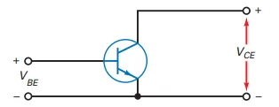
Transistor Equivalent Circuit Actual Transistor:
\(V_{BE}\): Voltage across the emitter-base junction.
\(V_{CE}\): Voltage across the collector-emitter terminals.
Transistor modeled as:
A diode at the base-emitter junction.
A current source at the collector side, where \(I_C = \beta_{dc} I_B\).
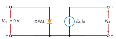
Ideal Approximation Features:
The emitter diode modeled as an ideal diode: \(V_{BE} = 0\).
Quick and simple calculation of base current: \[I_B = \frac{V_{BB}}{R_B}\] where \(V_{BB}\) is the base voltage supply, and \(R_B\) is the base resistor.
Collector Current: \[I_C = \beta_{dc} I_B\]
Usage:
Useful for troubleshooting and quick, rough approximations.
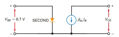
Second Approximation Features:
\(V_{BE} = 0.7 \, \text{V}\) for silicon transistors (\(V_{BE} = 0.3 \, \text{V}\) for germanium).
Accounts for the voltage drop of the emitter diode.
Base current calculation: \[I_B = \frac{V_{BB} - V_{BE}}{R_B}\]
Collector current: \[I_C = \beta_{dc} I_B\]
Usage:
Common in low-voltage circuits for improved accuracy over the ideal approximation.
Higher Approximations Bulk Resistance Effects:
At high currents, emitter diode resistance increases \(V_{BE}\): \[V_{BE} > 0.7 \, \text{V} \, (\text{e.g., up to } 1 \, \text{V})\]
Collector bulk resistance may also affect \(V_{CE}\) and \(I_C\).
Other Higher-Order Effects:
Leakage currents.
Early effect (variation of \(\beta_{dc}\) with \(V_{CE}\)).
Temperature dependence of parameters.
Recommendation:
Use computer simulations for calculations beyond the second approximation due to complexity.
Comparison of Approximations
| Approximation | Features | Accuracy | Use Case |
|---|---|---|---|
| Ideal | \(V_{BE} = 0\) | Low | Troubleshooting, rough calculations |
| Second | \(V_{BE} = 0.7 \, \text{V}\) (silicon) | Moderate | Most general-purpose circuits |
| Higher | Includes bulk resistances, Early effect | High (complex) | High-power or precision applications |
Key Takeaways
Approximations trade-off accuracy for simplicity:
Use ideal for quick estimates.
Use second for better accuracy in low-power circuits.
Rely on higher approximations or simulations for high-power or precision designs.
Emitter diode \(V_{BE}\):
\(0.7 \, \text{V}\) (silicon) is typical but increases with current in high-power circuits.
Bulk resistances and other effects:
Negligible in most low-power circuits, significant in high-power designs.
Introduction to the Load Line
Purpose: To set the DC operating conditions for a transistor to function as an amplifier or a switch.
Key Concept: Proper biasing of a transistor ensures stable operation.
Base Bias Example:
\(R_B = 1 \, \text{M}\Omega\), Base Current: \(I_B = 14.3 \, \mu \text{A}\).
\(\beta_{dc} = 100 \implies I_C = 1.43 \, \text{mA}\).
Collector-emitter voltage: \[V_{CE} = V_{CC} - I_C R_C = 15 \, \text{V} - (1.43 \, \text{mA})(3 \, \text{k}\Omega) = 10.7 \, \text{V}.\]
Quiescent (\(Q\)) Point: \[I_C = 1.43 \, \text{mA}, \, V_{CE} = 10.7 \, \text{V}.\]
The Graphical Solution
Load Line Equation: \[V_{CE} = V_{CC} - I_C R_C \implies I_C = \frac{V_{CC} - V_{CE}}{R_C}.\]
Definition:
The load line represents the relationship between \(I_C\) and \(V_{CE}\) for a given circuit.
It illustrates the impact of the load resistor (\(R_C\)) on transistor operation.
Graphing the Load Line
\[\begin{aligned} R_C &= 3 \, \text{k}\Omega, \, V_{CC} = 15 \, \text{V} \\ \textbf{Load Line Equation}:~I_C &= \frac{15 \, \text{V} - V_{CE}}{3 \, \text{k}\Omega}\\ V_{CE} = 0 \Rightarrow I_C & = \frac{15 \, \text{V}}{3 \, \text{k}\Omega} = 5 ~\text{mA} \\ I_C = 0 \Rightarrow V_{CE} & = 15 \, \text{V}. \end{aligned}\]
Visualizing the Load Line
Collector Curves:
Superimpose the load line on the transistor’s collector curves.
Interpretation:
The load line intersects the collector curves at different points, representing possible \(Q\) points.
The chosen \(Q\) point depends on the biasing conditions (\(I_B\) and \(V_{BE}\)).
The Quiescent (\(Q\)) Point
Definition:
The point of operation in the active region of the transistor where DC conditions are stable.
Example Calculation: \[I_C = 1.43 \, \text{mA}, \, V_{CE} = 10.7 \, \text{V}.\]
Significance:
Amplifiers operate best when the \(Q\) point is in the active region.
Key Takeaways
The load line graphically represents the transistor’s operation for given \(R_C\) and \(V_{CC}\).
The endpoints of the load line:
Upper end: \(I_C = 5 \, \text{mA}, \, V_{CE} = 0\).
Lower end: \(I_C = 0, \, V_{CE} = 15 \, \text{V}\).
The \(Q\) point is the steady-state operating condition where biasing sets \(I_C\) and \(V_{CE}\).
Proper biasing is crucial for ensuring stable and efficient transistor operation.
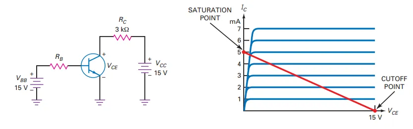
The Importance of the Load Line
Purpose: Represents all possible operating points of the circuit.
Key Insight:
As \(R_B\) varies from \(0\) to \(\infty\), \(I_B\) changes, resulting in changes in \(I_C\) and \(V_{CE}\) over their full ranges.
The load line is a graphical summary of these variations.
Visual Representation: The intersection of the load line with the transistor’s characteristic curves shows every possible operating point.
The Saturation Point
Definition: The point where the load line intersects the saturation region of the transistor curves.
Characteristics:
At saturation, \(V_{CE} \approx 0\).
\(I_C\) reaches its maximum possible value.
Approximation:
The saturation point is approximated as the upper end of the load line.
Example:
 \[I_C = \frac{15 \, \text{V}}{3 \,
\text{k}\Omega} = 5 \, \text{mA} \qquad I_{C(\text{sat})} =
\frac{V_{CC}}{R_C}\]
\[I_C = \frac{15 \, \text{V}}{3 \,
\text{k}\Omega} = 5 \, \text{mA} \qquad I_{C(\text{sat})} =
\frac{V_{CC}}{R_C}\]
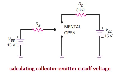
The Cutoff Point
Definition: The point where the load line intersects the cutoff region of the transistor curves.
Characteristics:
At cutoff, \(I_C \approx 0\).
\(V_{CE}\) reaches its maximum possible value.
Approximation:
The cutoff point is approximated as the lower end of the load line.
Example: \[V_{CE} = V_{CC} = 15 \, \text{V}.\]
Simple Process:
Visualize an open circuit between collector and emitter.
Comparing Saturation and Cutoff
| Operating Point | Condition | Collector Current (\(I_C\)) | Collector-Emitter Voltage (\(V_{CE}\)) | Load Line Position |
|---|---|---|---|---|
| Saturation | \(R_B \to 0\), \(I_B \to \infty\) | Maximum (\(I_{C(\text{sat})}\)) | Minimum (\(\approx 0\)) | Upper end |
| Cutoff | \(R_B \to \infty\), \(I_B \to 0\) | Minimum (\(\approx 0\)) | Maximum (\(V_{CE(\text{cutoff})} = V_{CC}\)) | Lower end |
Key Takeaways
Load Line: A visual summary of all possible transistor operating points.
Saturation Point:
Maximum \(I_C\), minimum \(V_{CE}\).
Found using: \[I_{C(\text{sat})} = \frac{V_{CC}}{R_C}.\]
Cutoff Point:
Minimum \(I_C\), maximum \(V_{CE}\).
Found using: \[V_{CE(\text{cutoff})} = V_{CC}.\]
Practical Insight: Understanding saturation and cutoff is essential for analyzing transistor behavior in switching and amplification applications.