Bipolar Junction Transistor (BJT)- Biasing
Importance of BJT Biasing for Amplification
Definition:
BJT biasing involves setting up a transistor amplifier for desired operating conditions.
Purpose:
Establish the DC operating point.
Ensure stability against variations like temperature changes.
Amplifier Analysis Components:
DC Analysis: Determines steady-state operating point.
AC Analysis: Determines response to input signals.
Superposition Principle: DC and AC analyses can be handled separately.
Energy Transfer:
AC signal amplification is powered by energy from DC supplies.
Interdependence:
DC operating point affects AC response and vice versa.
Biasing and its Significance
Biasing: Application of DC voltages to establish a fixed current and voltage level.
Q-Point (Quiescent Point): The operating point on device characteristics where the system is stable and inactive without a signal.
Purpose: Enables the transistor to amplify input signals effectively.
Real-World Use Cases:
Audio amplifiers
RF circuits
Signal processing applications
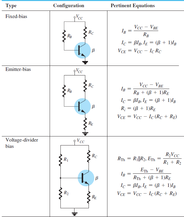
Common Biasing Techniques
Fixed-Bias
Emitter-Bias
Voltage-Divider Bias
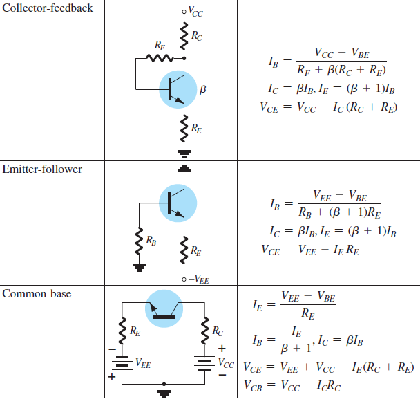
Collector Feedback
Emitter Follower
Common-Base
Revision of Important Facts
Basic Equations:
\(V_{BE} \approx 0.7 \, \text{V}\)
\(I_E = (\beta + 1) I_B \approx I_C\)
\(I_C = \beta I_B\)
Base current \(I_B\) is usually determined first.
Key Biasing Requirements for Amplification:
Forward bias for base-emitter junction.
Reverse bias for base-collector junction.
Maintain operation in the active region for effective signal processing.
Impact of Temperature:
Increases leakage current \(I_{CEO}\).
Alters current gain \(\beta_{ac}\).
Stability Factor \(S\):
Measures the effect of temperature on the Q-point stability.
Higher stability is desirable.
Q-Point Analysis
Operating Points:
Point A: Device completely OFF (unsuitable for amplification).
Point B: Ideal for small-signal amplification due to linear response.
Point C: Limited swing and nonlinear response.
Point D: High voltage operation, limiting positive voltage swing.
Importance of Point B for Amplification
Ensures uniform amplification over signal swing.
Maintains consistent device gain.
Maximized at Point B without crossing into cutoff or saturation.
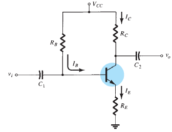
Fixed-Bias Configuration
Simplest DC bias configuration for a transistor.
- Can be applied to both NPN and PNP transistors by changing
current directions and voltage polarities.
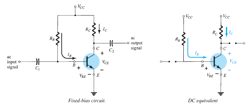
For DC Analysis AC sources are removed by replacing capacitors with open circuits.
- \[X_C = \frac{1}{2\pi f C}\]\(X_C = \infty \, \Omega\)\(f = 0\) is split into input and output sections to simplify analysis. Supply
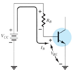
Base-Emitter Loop Analysis
- \[+V_{CC} - I_B R_B - V_{BE} = 0\]Kirchhoff’s Voltage Law (KVL):
- \[I_B = \frac{V_{CC} - V_{BE}}{R_B}\]Base Current Equation:
Key Insight: \(I_B\) is determined by \(R_B\) selection.
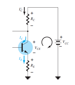
Collector-Emitter Loop Analysis
- \[I_C = \beta I_B\]Current Relationship:
- \[V_{CE} + I_C R_C - V_{CC} = 0 \quad \Rightarrow \quad V_{CE} = V_{CC} - I_C R_C\]KVL Application:
Observations: \(I_C\) is independent of \(R_C\) as long as the device remains in the active region. \(R_C\) affects the voltage \(V_{CE}\).
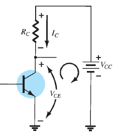
Important Relationships
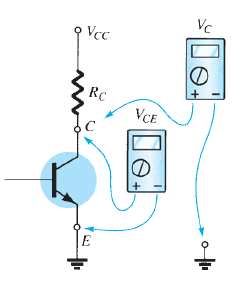
- \[V_{CE} = V_C - V_E = V_C\]Voltage Definitions:
Implications: \(V_E\) is often assumed as zero for simplicity. Control over \(V_{CE}\) is critical for setting the operating region.
Key Characteristics of Fixed-Bias Configuration
Simple to design and implement.
Provides control over base current through \(R_B\).
Sensitive to variations in \(\beta\) and temperature changes.
Primarily suited for low-power or stable environments.
Limitations and Stability Concerns
High sensitivity to temperature variations and transistor parameters.
Lack of automatic stabilization makes it less suitable for high-precision applications.
Improved configurations like voltage-divider bias address these concerns.
What is Saturation in Transistors?
Definition:
A system is in saturation when it operates at maximum levels.
Similar to a sponge fully soaked with water, unable to hold more.
In Transistors:
Current reaches a maximum for the design.
\(V_{CE}\) approaches or equals \(V_{CE_{\text{sat}}}\).
Base–collector junction no longer reverse-biased, leading to distortion.
Saturation Characteristics
\(V_{CE} \approx 0~\mathrm{V}\)
Collector current at maximum \(I_{C_{\text{sat}}}\).
High \(I_C\) and low voltage across collector-emitter terminals.
- Point where characteristic curves converge (Fig.).
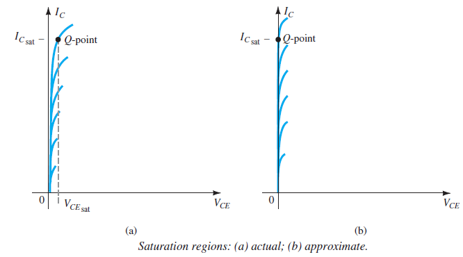
Treat the collector-emitter path as a short circuit.
Calculate the resulting \(I_C\) by assuming \(V_{CE} = 0~\mathrm{V}\).
\[R_{CE} = \frac{V_{CE}}{I_C} = \frac{0~\mathrm{V}}{I_{C_{\text{sat}}}} = 0~\Omega\]
Determining Saturation Current
Apply a short circuit between collector and emitter.
Voltage across \(R_C\) becomes \(V_{CC}\).
\[I_{C_{\text{sat}}} = \frac{V_{CC}}{R_C}\]\(I_C\) should remain below \(I_{C_{\text{sat}}}\) for linear amplification.
Importance of Avoiding Saturation
Distortion Risk:
Saturation disrupts linear amplification, introducing signal distortion.
Design Considerations:
Ensure \(I_C\) operates well below \(I_{C_{\text{sat}}}\) for clean amplification.
Practical Applications:
Avoiding saturation ensures consistent and accurate signal amplification.
Emitter-Bias Configuration
Objective: Improve stability over fixed-bias configuration.
Key Features:
Addition of emitter resistor \(R_E\).
Greater resistance to temperature variations and parameter shifts.
Application: Used for circuits requiring consistent performance under varying conditions.
\(R_E\) introduces feedback that stabilizes the circuit.
\(R_E\) impacts both base and collector-emitter loops.
Base–Emitter Loop Analysis
Compared to Fixed-Bias the additional term \((\beta + 1) R_E\) in the denominator improves stability.
Equivalent Circuit and Reflection Concept
\(R_E\) appears in base circuit as \((\beta + 1) R_E\) due to reflection effect.
Significantly larger apparent resistance due to \(\beta\) (50 or more).
\[\text{Input Resistance}~R_i = (\beta + 1) R_E\]Greater \(R_i\) offers better temperature stability and reduces sensitivity to variations in \(\beta\).

Collector–Emitter Loop Analysis

Voltage Levels and Biasing Points
Maintaining \(V_{CE}\) above saturation voltage ensures linear operation.
Proper selection of \(R_E\) and \(R_C\) determines \(V_{CE}\) and enhances stability.
Stabilizes operating point by providing negative feedback.
Ensures consistent operation despite changes in temperature or transistor parameters.
Voltage-Divider Bias
Biasing in BJTs sets the operating point (Q-point) for consistent performance.
Previous configurations depend on transistor’s current gain (\(\beta\)).
\(\beta\) is temperature-sensitive and varies, especially in silicon transistors.
Desire for bias circuits less dependent on \(\beta\).
Voltage-divider bias provides stable operating points despite \(\beta\) variations.
Proper circuit parameters lead to \(\beta\) independence for \(I_{CQ}\) and \(V_{CEQ}\).
Circuit Configuration

Resistors \(R_1\) and \(R_2\) form a voltage divider.
Bias point defined by \(I_{CQ}\) and \(V_{CEQ}\) stays stable.
Despite changes in \(\beta\), \(I_{CQ}\) and \(V_{CEQ}\) can remain fixed.
Analysis

\(V_E\), \(V_C\), and \(V_ B\) are same as obtained for the emitter-bias.
Benefits of Voltage-Divider Bias
Minimizes temperature and \(\beta\) sensitivity.
Stable Q-point ensures consistent circuit performance.
Versatile and widely used in practical designs.
Collector Feedback Configuration
An improved level of stability by introducing a feedback path from collector to base
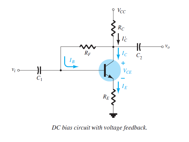
The Q-point is less sensitive to \(\beta\) and temperature changes than other biasing methods.
Base–Emitter Loop:
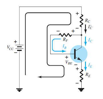 \[\begin{aligned} \text{KVL}~& V_{CC} - I_{C}^{\prime}R_C - I_BR_F - V_{BE} - I_ER_E =0 \\ &I_{C}^{\prime} = I_{C} + I_{B} \\ \text{Normally} ~& I_{C}^{\prime} \cong I_{C} = \beta I_B \quad I_E \cong I_{C} \\ \therefore ~ & V_{CC} - \beta I_B R_C - I_BR_F - V_{BE} - \beta I_B R_E =0 \\ \Rightarrow ~& I_B = \dfrac{V_{CC} - V_{BE} }{R_F + \beta (R_C + R_E)} \end{aligned}\]
- \[I_B = \dfrac{V^\prime}{R_F + \beta R^{\prime}}\]In general,
For fixed-bias configuration \(\Rightarrow~\beta R^\prime\) does not exist
For the emitter-bias \(\Rightarrow~\beta+1 \cong \beta \qquad R^\prime = R_E\)
- \[\begin{aligned} I_{CQ} & = \dfrac{\beta V^{\prime}}{R_F + \beta R^{\prime}} = \dfrac{V^\prime}{\dfrac{R_F}{\beta}+R^{\prime}} \\ &\cong \dfrac{V^\prime}{R^\prime}~ \left(\because R^\prime >> \dfrac{R_F}{\beta} \right) \\ \Rightarrow ~& \text{Independent of } \beta ~\text{variation} \end{aligned}\], Because
Collector–Emitter Loop:
 \[\begin{aligned} \text{KVL}~& I_ER_E + V_{CE} + I_C^{\prime}R_C - V_{CC} =0 \\ \Rightarrow~& I_C (R_C + R_E) + V_{CE} - V_{CC} = 0 ~(\because ~I_C^\prime \cong I_C \quad I_E \cong I_C ) \\ \Rightarrow~& V_{CE} = V_{CC} - I_C (R_C + R_E)\\ \Rightarrow~& \text{Exactly same as emitter-bias and voltage-divider bias} \end{aligned}\]
EMITTER-FOLLOWER CONFIGURATION
In collector-feedback, \(V_0\) is taken from collector terminal.
- In emitter-follower, the output is taken off the emitter
terminal.
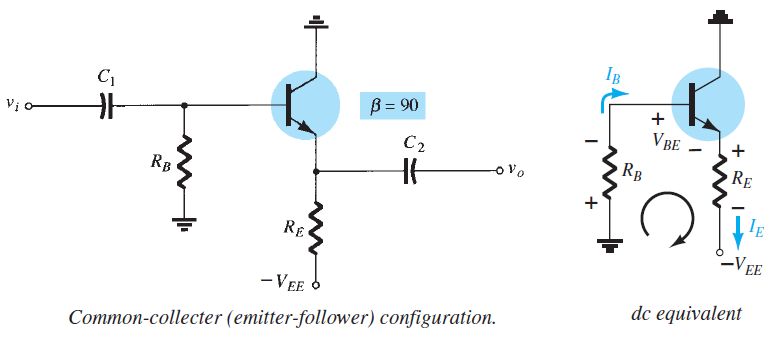 \[\begin{aligned} \text{KVL}\quad & -I_BR_B - V_{BE} -I_ER_E + V_{EE} = 0\\ \text{Using} \quad & I_E = (\beta+1)I_B \\ \Rightarrow~& I_BR_B + (\beta+1)I_BR_E = V_{EE} - V_{BE} \\ \Rightarrow~& I_B = \dfrac{V_{EE} - V_{BE}}{R_B + (\beta+1)R_E} \end{aligned}\]
 - \[V_{CE} = V_{EE} - I_E R_E\]Output network:
COMMON-BASE CONFIGURATION
Input signal is connected to the emitter terminal.
The base is held at ground or just above ground potential.
The common-base configuration is unique due to the use of two supplies and its design where the base is the common terminal.
Advantages: low input impedance, high output impedance, and good gain.
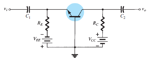
- \[\begin{aligned} & -V_{EE}+I_ER_E+V_{BE}=0 \\ & I_E=\frac{V_{EE}-V_{BE}}{R_E} \end{aligned}\]Input dc equivalent:
Determining \(V_{CE}\) and \(V_{CB}\):
\[\begin{aligned} &-V_{EE}+I_{E}R_{E}+V_{CE}+I_{C}R_{C}-V_{CC}=0\\ &I_{E}\cong I_{C} \\ &\boxed{V_{CE}=V_{EE}+V_{CC}-I_E(R_C+R_E)} \\ V_{CB}&=V_{CC}-I_{C}R_{C}\\ I_{C}&\cong I_{E} \\ & \boxed{V_{CB}=V_{CC}-I_CR_C} \end{aligned}\]
Summary