Bipolar Junction Transistor (BJT)- Amplifiers
Transistor Biasing and Small-Signal Amplifiers
Biasing of a transistor is purely a DC operation.
Purpose of biasing: Establish a Q-point for current and voltage variations in response to an AC input signal.
In applications requiring amplification of small signal voltages (e.g., from an antenna or microphone), variations around the Q-point are kept relatively small.
Amplifiers for these small AC signals are called small-signal amplifiers.
Linear Amplifier Operation and Transistor Behavior
A linear amplifier amplifies a signal without distortion, providing an exact amplified replica of the input.
In a voltage-divider biased transistor:
Coupling capacitors \(C_1\) and \(C_2\) block DC, preventing changes in the bias voltages at the base and collector.
The capacitors appear as shorts to the signal voltage.
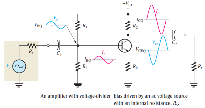
Sinusoidal AC source causes base voltage to vary around the DC bias \(V_{BQ}\).
The base current variation leads to a larger variation in collector current due to transistor current gain.
Collector voltage decreases as the collector current increases, and vice versa.
The collector-to-emitter voltage varies out of phase with the base voltage.
Phase inversion: There is always a phase shift between base and collector voltage.
Base Current and AC Load Line in a Linear Amplifier
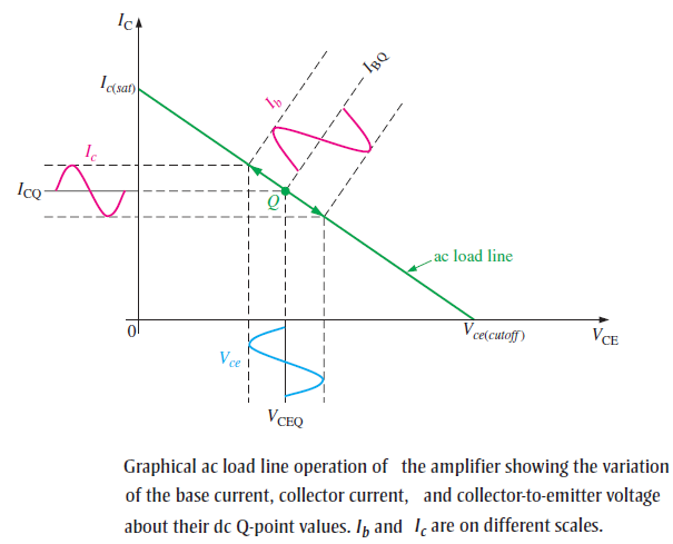
The sinusoidal voltage at the base produces a base current that varies above and below the Q-point along the AC load line.
Peak-to-peak variations in collector current and collector-to-emitter voltage are shown by lines projected from the peaks of the base current.
The AC load line differs from the DC load line:
The effective AC collector resistance is \(R_L\) in parallel with \(R_C\), which is less than the DC collector resistance \(R_C\) alone.
The distinction between the DC and AC load lines is explored further in the context of power amplifiers.
Transistor Models in Amplifier Circuits
Purpose: Represent the operation of a transistor in an amplifier using a model circuit.
Transistor Model Circuit: Utilizes internal transistor parameters to describe operation.
Types of Parameters:
r Parameters: Based on resistance values, commonly used to model transistor behavior.
h Parameters: An alternative system of parameters, briefly discussed.
- The five r parameters commonly used for BJTs are:
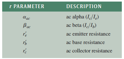
r-Parameter Transistor Model
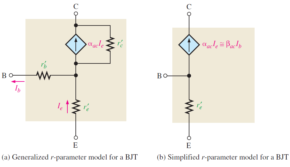
\(r_b^{\prime}\) is small enough to neglect \(\Rightarrow\) replaced by short
\(r_c^{\prime}\) usually several hundred \(\mathrm{k}\Omega\) \(\Rightarrow\) replaced by open
\(r_e^{\prime}\) is seen looking into the emitter of a F.B. transistor
Collector acts as a dependent current source of \(\alpha_{ac}I_e\) or \(\beta_{ac}I_b\)
\(r_e^{\prime}\) is the most important r-parameter
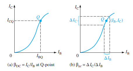
- \[\begin{aligned} \beta_{dc} & = \dfrac{I_C}{I_B}\\ \beta_{ac} & = \dfrac{\Delta I_C}{\Delta I_B}\\ \end{aligned}\]\(I_B\)\(I_C\)
h (hybrid) Parameters
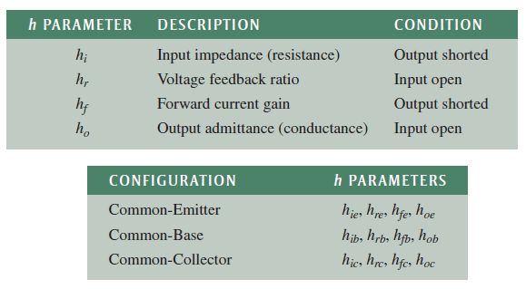
Parameters are relatively easy to measure
- \[\begin{aligned} \alpha_{ac}&=h_{fb}\\ \beta_{ac}&=h_{fe} \end{aligned}\]Relationships of h Parameters and r Parameters
- \[\begin{aligned}&{r'_e}=\frac{h_{re}}{h_{oe}}\\&r_{c}^{\prime}=\frac{h_{re}+1}{h_{oe}}\\&r_{b}^{\prime}=h_{ie}-\frac{h_{re}}{h_{oe}}(1+h_{fe})\end{aligned}\]-parameters can be obtained: parameters, so Datasheets often provide only common-emitter
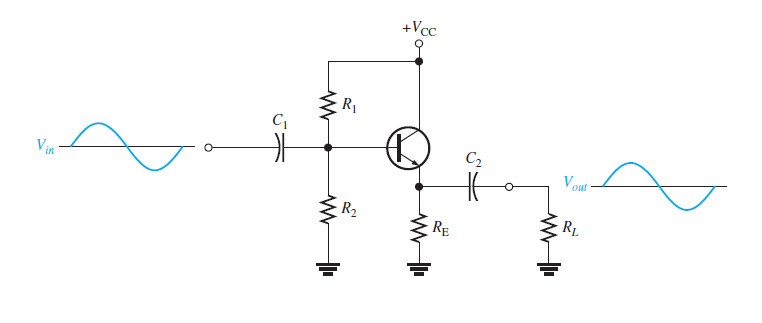
Common Emitter Amplifier
- Common-Emitter Amplifier with Voltage-Divider Bias
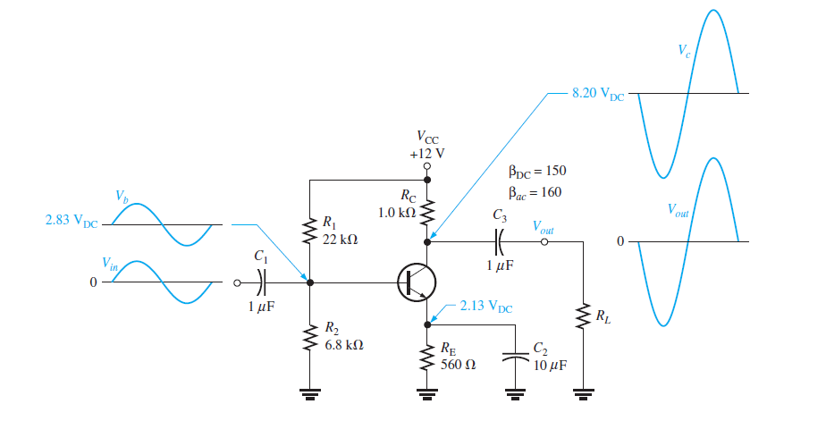
Coupling capacitors (\(C_1\) and \(C_3\)) for input and output
Bypass capacitor (\(C_2\)) from emitter to ground
Input Signal (Vin): Applied capacitively to the base terminal.
Output Signal (Vout): Taken capacitively from collector to load.
Emitter: Common to both the input and output signals.
Bypass Capacitor (C2): Shorts the emitter to ground at the signal frequency, ensuring no signal at the emitter.
Amplifiers operate in both ac and dc modes, but the common-emitter designation specifically refers to the ac operation.
The output signal is 180° out of phase with the input signal.
How Phase Inversion Occurs:
As \(V_{in}\) changes \(\Rightarrow\) \(I_B\) changes \(\Rightarrow\) \(I_C\) changes \(\Rightarrow\) deviates Q-point.
If \(I_B\uparrow \Rightarrow~I_C\uparrow \Rightarrow\) voltage drop across the collector resistor \(R_C~\uparrow\)
This leads to a decrease in the voltage at the collector.
Thus, a change in \(V_{in}\) causes the opposite change in the collector voltage, resulting in phase inversion.
Conclusion
The common-emitter amplifier provides voltage amplification and \(180^\circ\) phase inversion.
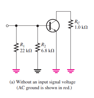
Determine DC bias values by removing AC components (coupling and bypass capacitors) since they appear open for DC.
Eliminate load resistor and signal source, not needed for DC analysis.
AC Signal Operation of an Amplifier
Capacitors as Shorts:
Capacitors \(C_1\), \(C_2\), and \(C_3\) are replaced by shorts as their values make the capacitive reactance (\(X_C\)) negligible at the signal frequency.
DC Source as Ground:
The DC source is replaced by ground in AC analysis because it has negligible internal resistance and does not produce an AC voltage, acting as an AC short.
AC Equivalent Circuit:
Both \(R_C\) and \(R_1\) are connected to AC ground, which is linked to \(V_{CC}\) in the actual circuit.
The bypass capacitor \(C_2\), which keeps the emitter at AC ground, making it the circuit’s common point.
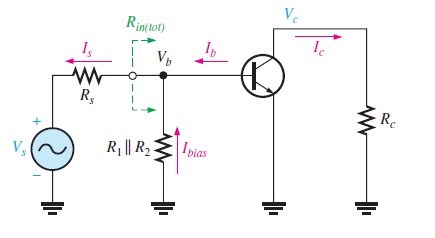
Signal (AC) Voltage at the Base
AC Voltage Source Connection:
When an AC source \(V_s\) is connected to the base, the base voltage depends on various resistances.
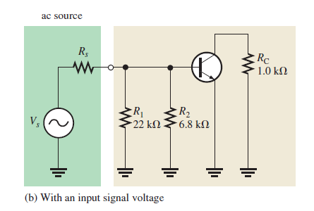
Factors Affecting Signal Voltage:
If the source’s internal resistance is \(0 \, \Omega\), the entire source voltage appears at the base.
With a nonzero internal resistance, three resistances must be considered:
Source Resistance (\(R_s\))
Bias Resistance (\(R_1 \parallel R_2\))
AC Input Resistance at the Base (\(R_{in(base)}\))
Total Input Resistance:
The total input resistance, \(R_{in(tot)}\), is the parallel combination of \(R_1\), \(R_2\), and \(R_{in(base)}\):
Voltage Divider Effect:
The source voltage, \(V_s\), is divided between \(R_s\) and \(R_{in(tot)}\), so the voltage at the base is given by:
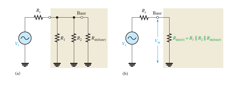
Special Case:
If \(R_s \ll R_{in(tot)}\), then \(V_b \approx V_s\).
This means the voltage at the base is nearly equal to the input voltage if the source resistance is much smaller than the total input resistance.
Design Trade-Offs:
High input resistance is desired to minimize signal loading.
Small resistances are necessary for stable biasing.
Achieving both high input resistance and stable biasing involves trade-offs in component selection.
Input Resistance at the Base
Use the simplified \(r\)-parameter model of the transistor to derive the AC input resistance at the base.
Output Resistance of Common-Emitter Amplifier
- \[R_{\text{out}} \approx R_C\]The output resistance of a common-emitter amplifier :
The more detailed expression is:
\[R_{\text{out}} = R_C \parallel r_c'\]is the internal AC collector resistance of the transistor. whereSince \(r_c' >> R_C\), the approximation is usually valid.
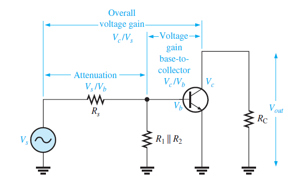
Voltage Gain
Equation represents Voltage gain (\(A_\nu\)) from base to collector .
Overall Amplifier Gain: from the source voltage to the collector, we must include the attenuation of the input circuit.
Attenuation: The reduction in signal voltage as it passes through a circuit, corresponding to a gain of less than 1.
Attenuation Example:
If the signal amplitude is reduced by half:
Attenuation = 2.
Gain = \(\frac{1}{\text{Attenuation}} = 0.5\).
Case Study:
Input signal: 10 mV.
Output signal: 2 mV.
Attenuation = \(\frac{10\,\text{mV}}{2\,\text{mV}} = 5\).
Gain = \(\frac{1}{5} = 0.2\).
Key Takeaways
Attenuation reduces the signal voltage as it passes through a circuit.
Attenuation and gain are inversely related:
The overall gain of the amplifier depends on both the voltage gain (\(A_\nu\)) and the attenuation of the input circuit.
Effect of Emitter Bypass Capacitor on Voltage Gain
\(C_2\) shorts AC signal around \(R_E\), maintaining emitter at AC ground.
- \[\text{Gain} = \frac{R_C}{r_e^{\prime}}\]Maximum gain achieved:
\(X_C\) must be very small compared to \(R_E\) across operating frequencies.
- \[10X_C \leq R_E \quad \text{at minimum operating frequency.}\]Rule-of-thumb:
Ensure \(X_C \approx 0\,\Omega\) for optimal performance.
Without Bypass Capacitor
Without a bypass capacitor, the emitter isn’t at AC ground.
- \[A_v=\frac{R_{\mathrm{C}}}{r_e^{\prime}+R_{\mathrm{E}}}\]\(R_E\)
Effect of a Load on the Voltage Gain
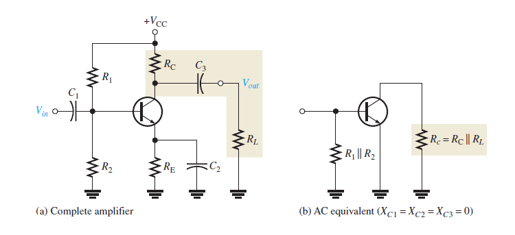
- \[R_c=\frac{R_\mathrm{C}R_L}{R_\mathrm{C}+R_L}\]The total ac collector resistance
- \[A_v=\frac{R_c}{r_e^{\prime}}\]with Replacing
- \[\begin{aligned} &R_c < R_C ~(\text{because of}~R_L) \Rightarrow A_v \downarrow \\ &R_L >> R_C \Rightarrow R_c \cong R_C \Rightarrow \text{very little effect of load} \end{aligned}\]If
Stability in Amplifiers:
Stability measures how well an amplifier maintains its design values over changes in temperature or transistor parameters (e.g., \(\beta\)).
- \[A_\nu = \frac{R_C}{r_e'} \Leftarrow r_e^\prime~ \text{changes, gain becomes unstable.}\]\(I_E\)\(r_e'\)\(A_\nu\)
- \[\begin{aligned} A_\nu & = \frac{R_C}{r_e' + R_E} \\ A_\nu & \approx \frac{R_C}{R_E} \qquad R_E \gg r_e' ~~ \text{(stable but lower gain)} \end{aligned}\]No Bypass Capacitor:
Swamping Technique
A compromise between fully bypassed and unbypassed \(R_E\).
Reduces the effect of \(r_e'\) on \(A_\nu\).
\(R_E\) is split into two resistors: \(R_{E1}\) (unbypassed) and \(R_{E2}\) (bypassed).
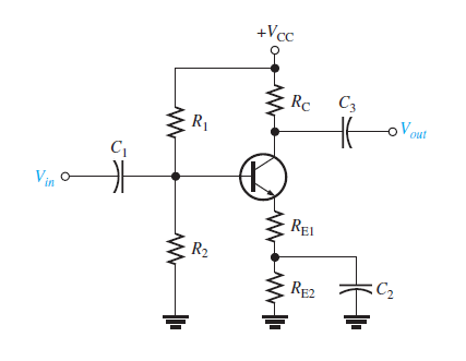
Both \(R_{E1}\) and \(R_{E2}\) affect DC bias , but only \(R_{E1}\) affects AC gain.
\[A_\nu = \frac{R_C}{r_e' + R_{E1}} \approx \frac{R_C}{R_{E1}} ~~ (R_{E1} \gg r_e')\]Achieves reasonable gain while maintaining stability.
- \[R_{in(base)}=\beta_{ac}(r_{e}^{\prime}+R_{\mathrm{E}1})\]Swamping increase the input resistance
Current Gain
 \[\begin{aligned} \text{base-to-collector~} \beta_{ac} &= \dfrac{I_c}{I_b} \\ \text{overall~} A_i &= \dfrac{I_c}{I_s} \\ I_s &= \dfrac{V_s}{R_s + R_{\text{in(tot)}}} \end{aligned}\]
- \[\begin{aligned} A_p & = A_v^\prime \cdot A_i \qquad (A_v^\prime=V_c/V_s) \end{aligned}\]Power Gain
Common-Collector (CC) Amplifier – Emitter-Follower (EF)
Voltage Gain: \(\approx 1\) (no significant amplification or phase inversion)
Input Resistance: High, suitable for impedance matching
Current Gain: High, useful for current amplification
Phase Inversion: None (output follows input)
The output voltage matches the input in both phase and amplitude, hence the term emitter-follower.
Input Signal: Applied to the base via a coupling capacitor
Output Signal: Taken from the emitter, also coupled via a capacitor
Collector: AC ground (no effect on AC signal)
Voltage Gain
\[\begin{aligned} V_{out} & =I_eR_e \\ V_{in} &=I_e(r_e^{\prime}+R_e) \\ A_\nu & =\dfrac{V_{out}}{V_{in}} =\frac{I_eR_e}{I_e(r_e^{\prime}+R_e)} =\frac{R_e}{r_e^{\prime}+R_e} <1 \quad (R_e = R_E || R_L) \\ A_{v}&\cong1 \quad (R_{e}>r_{e}^{\prime})\\ \end{aligned}\]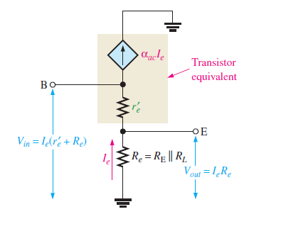
Input Resistance: High \(R_{in}\), making it a useful buffer circuit.
\[\begin{aligned} R_{in(base)} & =\frac{V_{in}}{I_{in}}=\frac{V_b}{I_b}=\frac{I_e(r_e^{\prime}+R_e)}{I_b} \\ &\cong\frac{\beta_{ac}I_b(r_e^{\prime}+R_e)}{I_b} \quad (I_e\cong I_c=\beta_{ac}I_b) \\ &\cong\beta_{ac}(r_{e}^{\prime}+R_{e}) \\ &\cong\beta_{ac}R_{e} \quad (\text{if}~ R_{e}>r_{e}^{\prime}) \\ R_{in(tot)} & =R_1\parallel R_2\parallel R_{in(base)} \end{aligned}\]- \[R_{out}\cong\left(\frac{R_s}{\beta_{ac}}\right)\parallel R_\mathrm{E}\]Output Resistance:
- \[\begin{aligned} & A_i=\frac{I_e}{I_{i n}} \quad (I_{i n}=V_{i n} / R_{\text {in }(t o t)} .)\\ & A_p=A_v A_i \cong A_i \quad (A_v \cong 1) \end{aligned}\]Current and Power Gain
The Darlington Pair
\(\beta_{ac}\) is a major factor in determining the \(R_{in}\) of an amplifier.
Higher \(\beta_{ac}\) improves the input resistance.
- Two transistors connected in Darlington configuration.
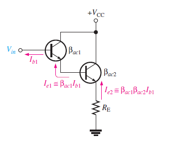
First transistor emitter current: \(I_{e1} \approx \beta_{ac1} I_{b1}\)
Second transistor emitter current: \(I_{e2} \approx \beta_{ac2} I_{e1} = \beta_{ac1} \beta_{ac2} I_{b1}\)
The effective current gain for the Darlington pair: \(\beta_{ac} = \beta_{ac1} \beta_{ac2}\)
Input resistance: \(R_{in} = \beta_{ac1} \beta_{ac2} R_{\mathrm{E}}\)
Assumption: \(r_e' \ll R_\mathrm{E}\) for simplification.
Application:
A common-emitter amplifier with a 1.0 k\(\Omega\) collector resistor (R\(_C\)) must drive a low-resistance load (8\(\Omega\) speaker).
The speaker is capacitively coupled to the amplifier’s output, causing the load to appear in parallel with the collector resistor.
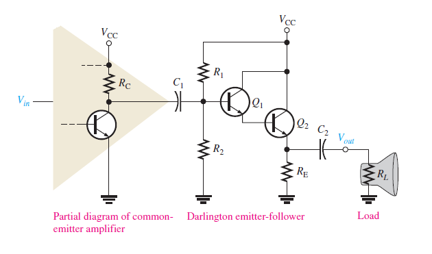
- \[R_c = R_C \parallel R_L = 1.0\ \text{k}\Omega \parallel 8\ \Omega = 7.94\ \Omega\]Parallel Resistance Calculation:
Impact on Voltage Gain:
Without load:
With 8\(\Omega\) speaker load:
Conclusion: The voltage gain is significantly reduced due to the low resistance of the speaker.
Solution: Use an emitter-follower configuration with a Darlington pair to buffer the amplifier and speaker, restoring voltage gain and preventing excessive loading.
COMMON-BASE AMPLIFIER
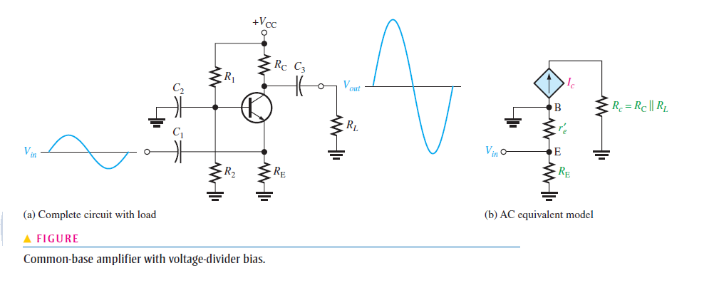
Provides high voltage amplification.
Maximum current gain is limited to 1.
Low input resistance making it ideal for certain applications.
Optimal for Low-Resistance Sources :
Note: \(A_\nu\) same as for the common-emitter amplifier, but no phase inversion from emitter to collector.
Cascaded amplifiers
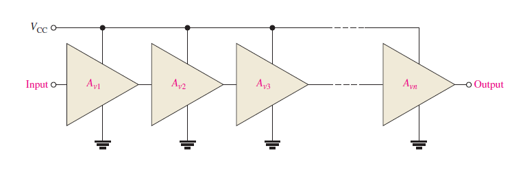
- \[A_{\nu}^{\prime}=A_{\nu1}A_{\nu2}A_{\nu3}\ldots A_{\nu n}\]The overall voltage gain of n-cascaded amplifiers:
- \[A_{\nu(\mathbf{dB})}=20\log A_{\nu}\]Amplifier voltage gain is often expressed in decibels (dB) as follows:
- \[A_{\nu(\mathrm{dB})}^{\prime}=A_{\nu1(\mathrm{dB})}+A_{\nu2(\mathrm{dB})}+\cdots+A_{\nu n(\mathrm{dB})}\]The total voltage gain in dB is the sum of individual gains.
Differential Amplifier
A differential amplifier produces an output based on the difference between two input voltages.
It has two modes of operation:
Differential mode: Inputs are different.
Common mode: Inputs are the same.
It is key in operational amplifiers.
- It has two inputs and two outputs.
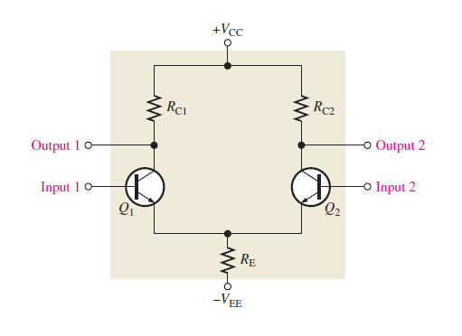
Basic operation of a differential amplifier:
Both inputs grounded:
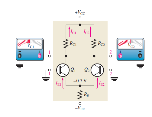
Bias voltage on input 1 with input 2 grounded:
Q1:
\(V_B\) increases \(\rightarrow I_{\mathrm{C1}}\) increases
Emitter voltage: \(V_{\mathrm{E}} = V_{\mathrm{B}} - 0.7\:\mathrm{V}\)
Q2:
Base at 0V \(\rightarrow\) Reduced forward bias \(\rightarrow I_{\mathrm{C2}}\) decreases
Results:
\(I_{\mathrm{C1}}\) increases \(\rightarrow V_{\mathrm{C1}}\) decreases
\(I_{\mathrm{C2}}\) decreases \(\rightarrow V_{\mathrm{C2}}\) increases
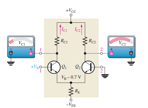
Bias voltage on input 2 with input 1 grounded
The positive bias voltage causes \(Q_2\) to conduct more, resulting in an increase in \(I_{C2}\).
The emitter voltage of \(Q_2\) is raised.
Impact on Q1:
The raised emitter voltage reduces the forward bias of \(Q_1\) (since its base is held at ground).
This causes a decrease in \(I_{C1}\).
Final Outcome:
The increase in \(I_{C2}\) results in a decrease in \(V_{C2}\).
The decrease in \(I_{C1}\) results in an increase in \(V_{C1}\).
Modes of Signal Operation:
Single-Ended Differential Input
Double-Ended Differential Input
Common-Mode Input
Key role: Amplify desired signals while rejecting unwanted noise.
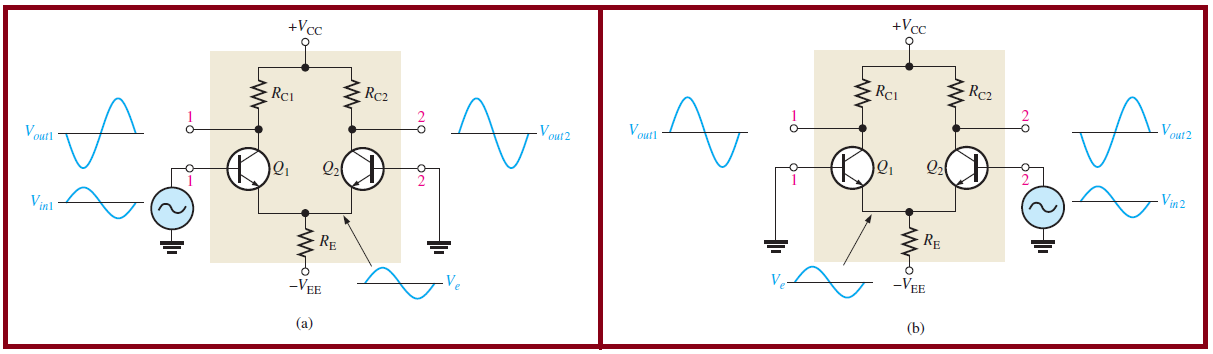
Single-Ended Differential Input
One input grounded, signal applied to the other.
Two cases:
Signal applied to Input 1:
Inverted, amplified signal at Output 1.
Noninverted, amplified signal at Output 2.
Signal applied to Input 2:
Inverted, amplified signal at Output 2.
Noninverted, amplified signal at Output 1.
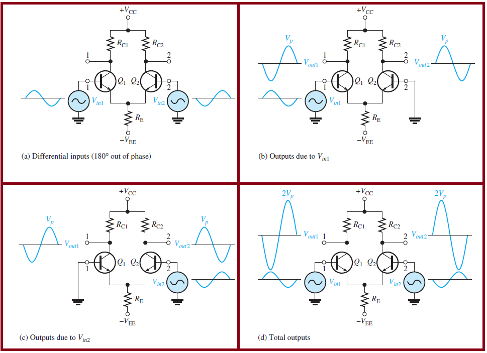
Double-Ended Differential Inputs
Two opposite-polarity (out-of-phase) signals applied to both inputs.
Each input affects the output:
Input 1 alone produces certain output signals.
Input 2 alone produces another set of output signals.
Superimposing both results in final output signal.
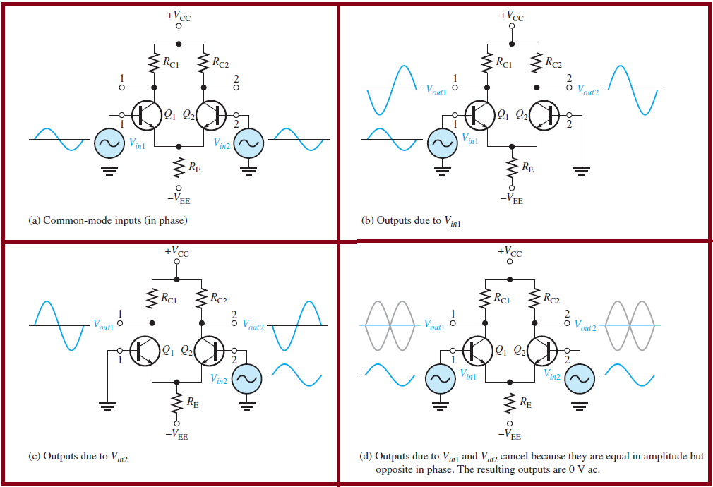
Common-Mode Inputs
Identical signals (same phase, frequency, and amplitude) applied to both inputs.
Individual input effects:
Input 1 alone produces signals of opposite polarity at outputs.
Input 2 alone does the same.
When both signals are applied, they cancel each other out.
Importance of Common-Mode Rejection
Eliminates unwanted signals (noise) appearing on both inputs.
Noise sources:
Radiated energy from adjacent lines.
60 Hz power line interference.
Other electromagnetic sources.
Enhances signal integrity in communication and instrumentation applications.
Common-Mode Rejection Ratio (CMRR)
Desired signals appear on only one input or with opposite polarities on both inputs.
These desired signals are amplified and appear on the outputs.
Unwanted signals (noise) appearing with the same polarity on both inputs are canceled.
- \[\mathrm{CMRR} = \frac{A_{v(d)}}{A_{c m}}\]The measure of an amplifier’s ability to reject common-mode signals is the Common-Mode Rejection Ratio (CMRR):
A high CMRR means high differential gain and low common-mode gain.
- \[\mathrm{CMRR} = 20 \log \left(\frac{A_{v(d)}}{A_{c m}}\right)\]CMRR is often expressed in decibels (dB):