Demonstrative Video
Contents
Fundamentals of a Transistor
Construction and operation of NPN and PNP transistors
Biasing of BJT: CB, CE and CC configuration
Characteristics of CB, CE, CC configuration
Fundamentals
W. Shockley, J. Barden, & W. Brattain invented transistor in 1947.
Transistor \(\Rightarrow\) transfer + resistor \(\Rightarrow\) transfer of an input signal from a low resistance circuit to a high resistance circuit.
A three-terminal semiconductor device: emitter (E), base (B), and collector (C).
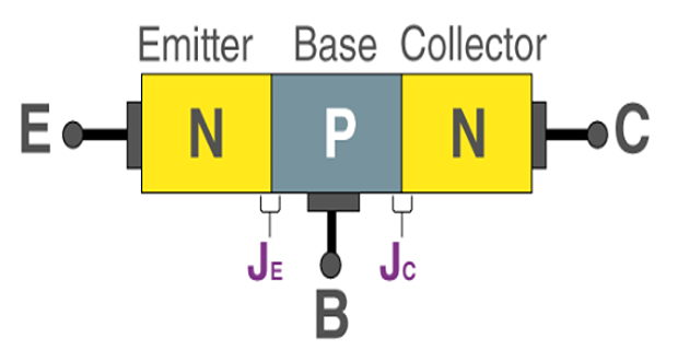
It consists of two p-n junctions: the E-B and B-C junctions.
It is capable of amplifying or magnifying a signal.
The BJT is a current controlled device.
When a small amplitude signal is applied to the base, it is amplified and available at the collector.
Requires an external DC source for the amplification process.
Construction
BJT is typically made using doped silicon or germanium.
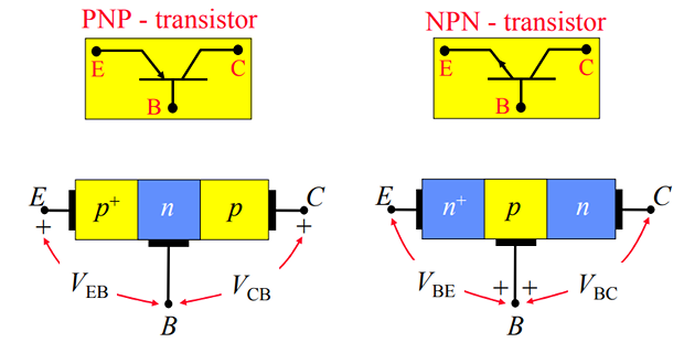
Doping : Emitter (heavily), base (lightly), and collector (moderately).
Each layer thickness determines the performance of the transistor.
PNP/ NPN transistors have very closely spaced pn-junctions.
The base must be small to allow interaction between the two pn-junctions.
The flow of charge in a BJT is due to the diffusion of charge carriers between the two regions belonging to different charge concentrations.
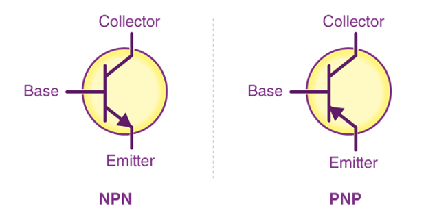
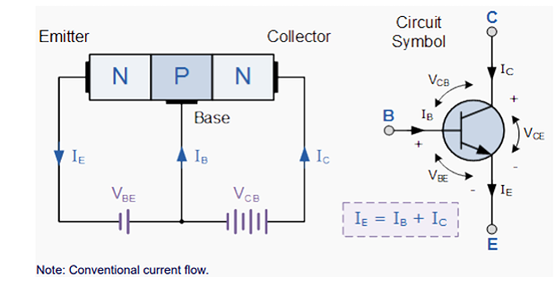
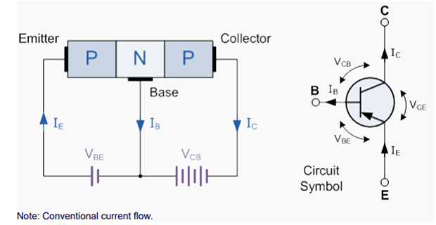
The base-emitter junction is forward biased, and the base-collector junction is reverse biased.
Forward biased means p-doped region has more potential than the n-doped side.
NPN and PNP Transistors
NPN
PNP
Properties of BJT
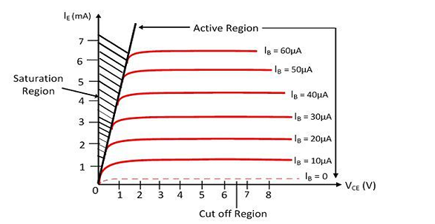
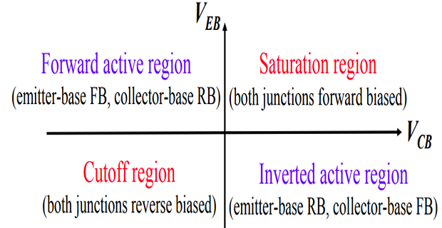
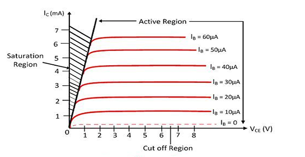
There are three operating regions of a BJT:
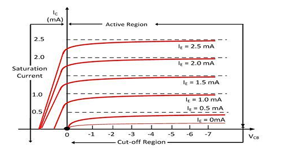
Active region: operate as an amplifier.
Saturation region: is fully on and operates as a switch such that collector current is equal to the saturation current.
Cut-off region: is fully off and collector current is equal to zero.
For ex - PNP
The Biased Transistor
Biased
transistor
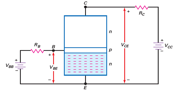
An unbiased transistor is like two back-to-back diodes
Heavily doped emitter inject its free electrons into the base.
Emitter injects free e
into base
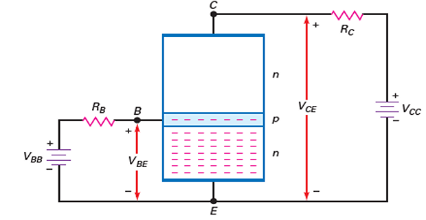
Lightly doped base pass emitter-injected electrons on to the collector.
Free e from base flow
into collector
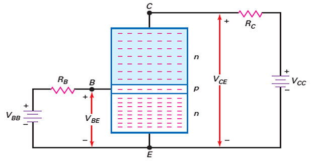
Collector collects most of the electrons from the base.
Transistor currents
The emitter terminal, being the source of electrons, carries the largest current.
As most of the emitter electrons flow towards the collector, the collector current is nearly equal to the emitter current.
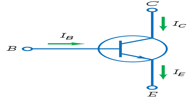
npn-transistor
Base current is significantly smaller, often less than 1% of the collector current.
\[\begin{aligned} &\boxed{I_E = I_C + I_B}~\Leftarrow~\text{KCL} \\ I_C & \approx I_E \\ I_B & << I_C \end{aligned}\]
Current gain in transistor
The dc alpha is defined as the dc collector current divided by the dc emitter current:
\[\boxed{\alpha = \dfrac{I_C}{I_E}}\]
Low-power transistor, \(\alpha>0.99\) and high-power transistor \(\alpha>0.95\)
The dc beta is defined as the ratio of the dc collector current to the dc base current:
\[\boxed{\beta = \dfrac{I_C}{I_B}}\]
The current gain is a significant advantage of a transistor and has paved the way for various applications.
Low-power transistors (under 1 W) \(\Rightarrow\) current gain 100 to 300.
High-power transistors (over 1 W) \(\Rightarrow\) current gain 20 to 100.
Relationship between \(\alpha\) and \(\beta\)
\[\boxed{\alpha = \dfrac{I_C}{I_E} = \dfrac{\beta}{1+\beta}}\] \[\boxed{\beta = \dfrac{I_C}{I_B} = \dfrac{\alpha}{1-\alpha}}\]
Derivation
\[\begin{aligned} I_E & = I_B + I_C \\ \Rightarrow~\dfrac{I_E}{I_C} & = \dfrac{I_B}{I_C}+1\\ \Rightarrow~\dfrac{1}{\alpha} & = \dfrac{1}{\beta}+1\\ \Rightarrow~&\boxed{\alpha = \dfrac{\beta}{1+\beta}} \end{aligned}\]
Relating formulas
\[\begin{aligned} I_E & = \dfrac{I_C}{\alpha} = I_B \cdot (1+\beta) \\ I_C & = \beta \cdot I_B = \alpha \cdot I_E\\ I_B & = \dfrac{I_C}{\beta} = \dfrac{I_E}{1+\beta} = I_E \cdot (1-\alpha) \end{aligned}\]
BJT Configurations
Since BJT has three leads, there are three possible amplifier types:
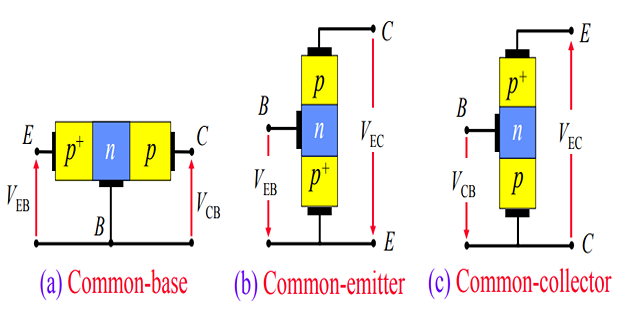
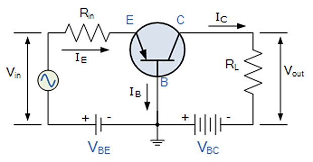
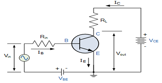
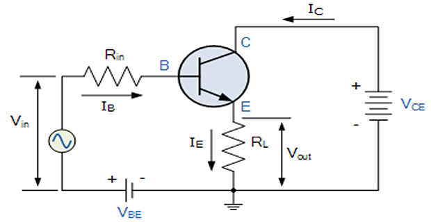
Common-Base \[\begin{aligned}
\text{Voltage gain}~A_v & = \dfrac{V_{out}}{V_{in}}=
\dfrac{I_C \times R_L}{I_E \times R_{in}}
\end{aligned}\]

Common-Emitter
\[\begin{aligned}
\alpha & = \dfrac{I_C}{I_E} \qquad \beta = \dfrac{I_C}{I_B}\\
I_E & = I_C+I_B\\
\alpha & = \dfrac{\beta}{\beta+1} \quad \beta -
\dfrac{\alpha}{1-\alpha}
\end{aligned}\]

Common-Collector
\[\begin{aligned}
A_i & = \dfrac{I_E}{I_B}
= \dfrac{I_C+I_B}{I_B}\\
& = \dfrac{I_C}{I_B}+1
= \beta +1
\end{aligned}\]

Comparison of BJT Configurations
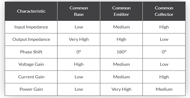
Characteristics of the main configurations :
Common Emitter – has both voltage and current gain
Common Collector – has no voltage gain but has a current gain
Common base – has no current gain but has a voltage gain
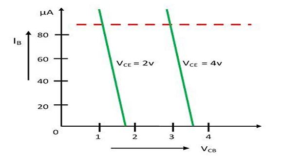
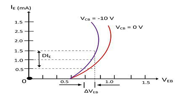
Input & Output Characteristics
Common Base
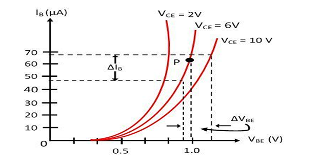
Common Emitter
Common Collector
